-
Notifications
You must be signed in to change notification settings - Fork 10
Cypress FX2 based Logic Analyzers
Development boards based on the Cypress (now Infineon) FX2 chipset (the CY7C68013A) are widely available for ~£10-£20. These boards can be used as cheap 8-bit/16 bit USB logic analyzers.
One use of such a logic analyer is in debugging 8-bit microprocessor based computer systems. The logic analyzer is setup to capture the microprocessor data bus, and optionally a small number of control signals. Software can then be used to post-process the binary data into a human readable form, showing the instructions executed and the machine state.
???? :          : RESET !!       : A=?? X=?? Y=?? SP=?? N=? V=? D=? I=1 Z=? C=?
Rd:   D9CD = A9
Rd:   D9CE = 40
D9CD : A9 40    : LDA #40        : A=40 X=?? Y=?? SP=?? N=0 V=? D=? I=1 Z=0 C=?
Rd:   D9CF = 8D
Rd:   D9D0 = 00
Rd:   D9D1 = 0D
Wr:   0D00 = 40
D9CF : 8D 00 0D : STA 0D00       : A=40 X=?? Y=?? SP=?? N=0 V=? D=? I=1 Z=0 C=?
Rd:   D9D2 = 78
D9D2 : 78       : SEI            : A=40 X=?? Y=?? SP=?? N=0 V=? D=? I=1 Z=0 C=?
Rd:   D9D3 = D8
D9D3 : D8       : CLD            : A=40 X=?? Y=?? SP=?? N=0 V=? D=0 I=1 Z=0 C=?
Rd:   D9D4 = A2
Rd:   D9D5 = FF
D9D4 : A2 FF    : LDX #FF        : A=40 X=FF Y=?? SP=?? N=1 V=? D=0 I=1 Z=0 C=?
Rd:   D9D6 = 9A
D9D6 : 9A       : TXS            : A=40 X=FF Y=?? SP=FF N=1 V=? D=0 I=1 Z=0 C=?
Rd:   D9D7 = AD
Rd:   D9D8 = 4E
Rd:   D9D9 = FE
Rd:   FE4E = 80
D9D7 : AD 4E FE : LDA FE4E       : A=80 X=FF Y=?? SP=FF N=1 V=? D=0 I=1 Z=0 C=?
There are instruction decoders available for several populat microprocessors:
- 6502 Decoder (which also supports the 65C02 and the 65C816)
- 6809 Decoder (which also supports the 6309)
- Z80 Decoder
This page covers the differences between the FX2 analyzer boards that are commonly available (in 2023):
The page also gives some guidance on the tools that can be used to capture data:
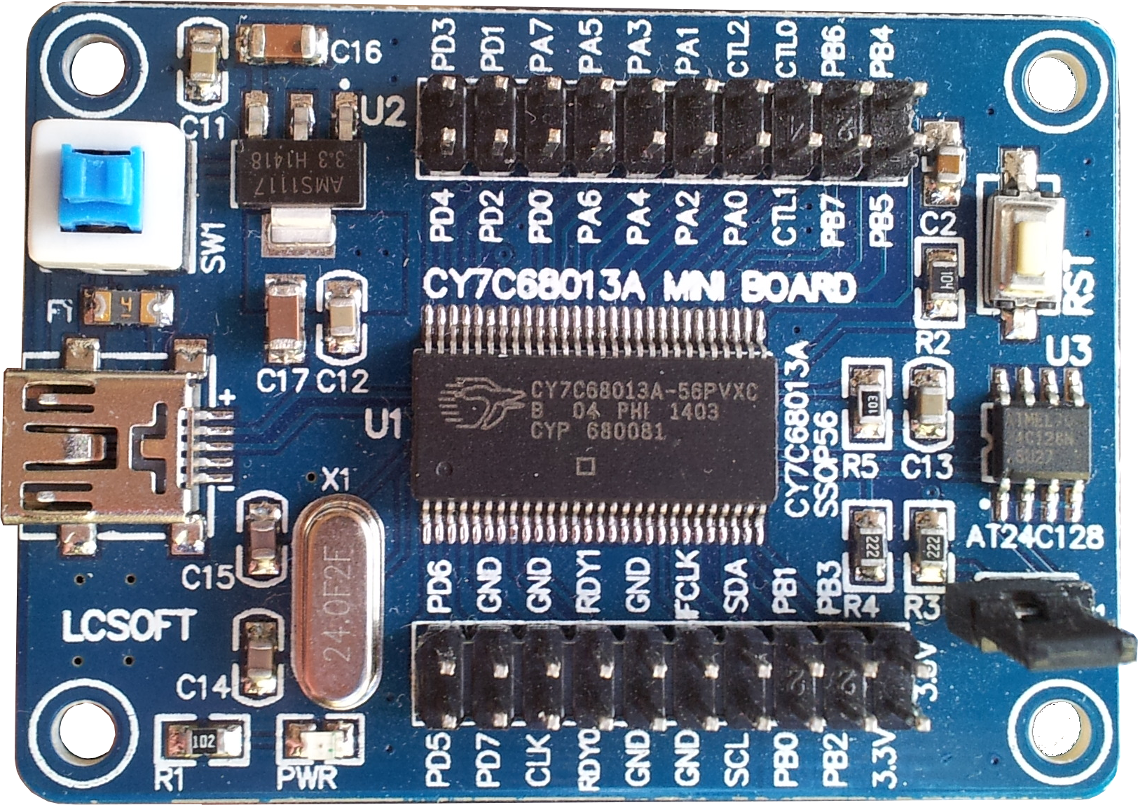
This board is branded LCSOFT on the silk screen, has one jumper, and has the reset button on the opposite side to the USB connector:

References:
The jumper J1 connects the A0 input of the EEPROM to VCC:
- when the jumper is fitted, the USB Vendor/Product ID is read from the EEPROM
- when the jumper is missing, the USB Vendor/Product ID defaults to 04b4:8613.
I prefer to remove this jumper, as the contents of the EEPROM are supplier specific, and can affect the operation of the board. However, the default ID 04b4:8613 is often claimed by a diagnostic module called usbtest, which prevents fx2pipe working. So you need to make sure the usbtest module is blacklisted by your kernel. On Ubuntu, you add the following line to /etc/modprobe.d/blacklist.conf
# The USBtest module, interferes with fx2pipe
blacklist usbtest
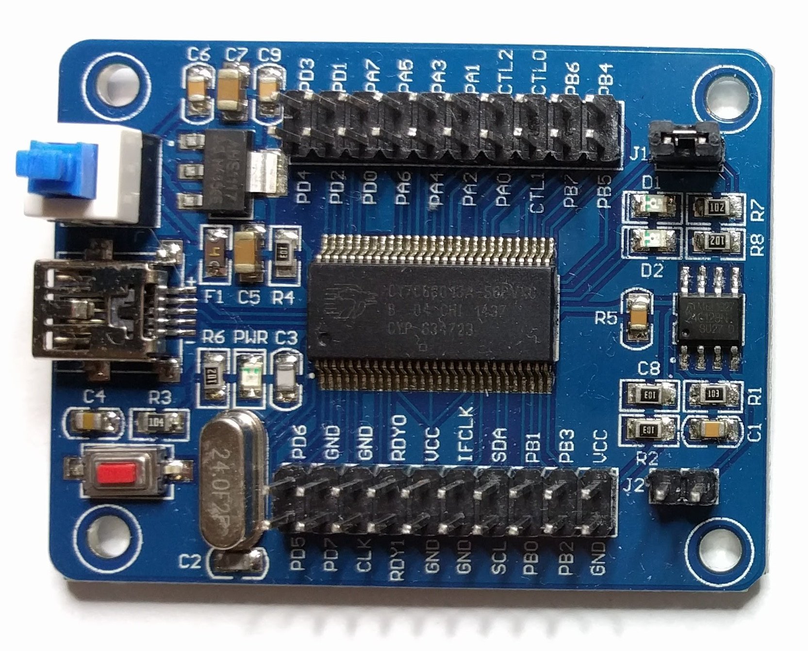
This board is unbranded on the silk screen, has two jumpers, and has the reset button on the same side as the USB connector:

References:
There are a number of differences between the Geeetech and LCSoft boards:
Connector differences:
- There is one connector pin that is 3V3 on the LCSoft board, and GND on the Geeetech board. If you are designing an adapter for the FX2 board, it's best to leave tis pin unconnected.
- There is an error on the silk-screen: the labels RDY0 and RDY1 are swapped. So the external clock needs to be connected to the pin labelled RDY0, not RDY1. This pin is in the same physical position on both board.
Jumper J1 on the Geetech board connects the anodes of LEDs D1/D2 to 3V3. These LEDs are connected to PA0 and PA1. The setting of this jumper should not matter.
Jumper J2 connects the A0 input of the EEPROM to GND:
- when the jumper is missing, the USB Vendor/Product ID is read from the EEPROM
- when the jumper is fitted, the USB Vendor/Product ID defaults to 04b4:8613.
This jumper must be fitted, otherwise captures from fx2pipe will not work. We don't currently understand what configuration data in the EEPROM is interfering with fx2pipe. But user gfoot on 6502.org found this was indeed the case. See here
The open source Sigrok software includes support for the FX2 analyzer.
Sigrok builds are available on Windows, Linux and MacOS.
Here'e an example sigrok-cli command:
sigrok-cli -d fx2lafw --config samplerate=12MHz -o data.bin -O binary --continuous
To limit the number of channels, add:
--channels D0,D1,D2,D3,D4,D5,D6,D7
To capture a fixed number of samples, e.g. 10 million, replace --continuous with
--samples 10M
To trigger on one of the inputs, e.g. the rising edge of D14 (normally connected to nRST):
--trigger D14=r
When capturing with Sigrok, the FX2 analyzer always samples data using it's own internal clock. So data bus samples are asynchronous to the microprocessor clock. Consequently, it's necessary to sample at a much higher frequency than the microprocessor clock (over-sampling) to get an error-free trace.
There is no hard and fast rule as to what over-sampling factor is necessary for a reliable instruction trace. This is actually system dependent, as it depends on how long the 6502 data bus is stable before the falling edge of Phi2. In a BBC micro, with a 2MHz 6502, it's typically necessary to sample at 12MHz to get an error-free trace.
The sigrok also supports a relatively limited set of sample rates, for example: 1MHz, 2MHz, 3MHz, 4MHz, 6MHz, 8MHz, 12MHz, 24MHz.
For these reason, I prefer to use a different capture tool: fx2pipe.
fx2pipe is an an open source project developed by Wolfgang Wieser. The original web page is here: http://www.triplespark.net/elec/periph/USB-FX2/software/fx2pipe.html
When capturing with fx2pipe there is more flexibility in how the FX2 analyzer is configured. It's possible to configure the FX2 analyzer to capture data using an external clock. Capturing on either the positive or negative edge is possible.
I would recommend using the version of fx2pipe in the 6502Decoder repository, as this has a couple of improvements on the original. https://github.com/hoglet67/6502Decoder/tree/master/fx2pipe
Note: fx2pipe relies on an older version of libusb: libusb-0.1 - it will NOT work with libusb-1.0, nor with libusb-compat-0.1.
To build fx2pipe:
cd 6502Decoder/fx2pipe
./configure
make
sudo make install
This will install fx2pipe to /usr/local/bin
You can see all the options available with:
$ fx2pipe --help
USAGE: fx2pipe [option|assignment]...
Long options:
  --help       print this
  --version    print version information
Short options: (Can be compined into single option)
  -i           run in IN direction, i.e. read data from USB EP6 (default)
  -o           run in OUT direction, i.e. write data to USB EP2
  -0           no stdio; send NULs / throw away read data (for timing)
  -8,-w        use 8bit / 16bit (default) wide fifo bus on FX2 side
  -2,-3,-4     use double, triple or quad (default) buffered FX2 fifo
  -s,-a        run in sync (default) / async slave fifo mode
  -O,-I        shortcut for -o0, -i0, respectively
Assignments: (Leading '-' can be left away)
  -d=NN        use n-th (unconfigured) FX2 device (start with NN=0, default)
  -d=VID:PID[:N] use N-th device with specified VID and PID
  -n=NNN       stop after NNN bytes; suffix k,M,G for mult. with 2^10,20,30
  -bs=NNN      set IO block size to NNN, max 16384 (default 16384)
  -ps=NN       set pipeline size (number of URBs; default 16)
  -sched=P[,N] set scheduling policy P ("fifo" or "rr") and prio N
  -fw=PATH     use specified firmware IHX file instead of built-in one
               omit path to not download any firmware (just reset device)
  -ifclk=[x|30[o]|48[o]][i] specify interface clock:
               x -> external; 30,48 -> internal clock 30/48MHz, suffix 'o'
               to enable output to IFCLK pin, 'i' to invert IFCLK
  -cko=[12|24|48][o|z][i] specify 8051 frequency in MHz (default: 48) and
               CLKOUT pin: output 'o' (default), tristate 'z', invert 'i'

fx2pipe - pipe data in or out of an Cypress FX2 device (CY7C6801x[A])
          Copyright (c) 2006--2011 by Wolfgang Wieser; License: GPL
These optionas generally take sensible defaults.
There are two modes supported by fx2pipe that allow the use of an external clock:
The external clock is connected to the RDY1 input of the FX2 (please note, on the Geeetech board the RDY0 and RDY1 labels are swapped).
The following command line is used:
fx2pipe -a > data.bin
With the (modified) version of fx2pipe in this repository, this will capture on the falling edge of the clock. To capture on the rising edge, you need to add --ifclk=i to invert the sense of the clock.
To use this mode, the inputs of the FX2 analyzer should be connected as follows:
- PB7..0 are the lower 8 bits of data input
- PD7..0 are the upper 8 bits of data input (16 bit wide mode only)
- IFCLK z
- RDY0 (SLRD) tie to 3V3 with a 1K resistor
- RDY1 (SLWR) is the external clock, which should be less than 7MHz
- PA2 (SLOE) tie to 3V3 with a 1K resistor
- PA4 (FIFOADR0) tie to GND a 1K resistor
- PA5 (FIFOADR0) tie to 3V3 with a 1K resistor
It's best to explicitely tie these pins to GND/3V3 via resistors, as many of the pins are bidirectional. That said, I generally omit the pullups (as unconnected inputs seem to float high), and make the connections to GND directly.
The external clock is connected to the IFCLK input of the FX2.
The following command line is used:
fx2pipe -s -ifclk=xi > data.bin
This will capture on the falling edge of the clock. To capture on the rising edge, you need to use --ifclk=x to invert the sense of the clock.
To use this mode, the inputs of the FX2 analyzer should be connected as follows:
- PB7..0 are the lower 8 bits of data input
- PD7..0 are the upper 8 bits of data input (16 bit wide mode only)
- IFCLK is the external clock, which must be between 5MHz and 48MHz
- RDY0 (SLRD) tie to 3V3 with a 1K resistor
- RDY1 (SLWR) tie to GND (if -ifclk=xi) or 3V3 (if -ifclk=x) with a 1K resistor
- PA2 (SLOE) tie to 3V3 with a 1K resistor
- PA4 (FIFOADR0) tie to GND a 1K resistor
- PA5 (FIFOADR0) tie to 3V3 with a 1K resistor
It's best to explicitely tie these pins to GND/3V3 via resistors, as many of the pins are bidirectional. That said, I generally omit the pullups (as unconnected inputs seem to float high), and make the connections to GND directly.
In practice the maxiumum clock speed is limited by the USB-2 transfer rate, and the data width. In 16-bit mode the limit appears to be 20MHz. In 8-bit mode the limit is 40MHz. This value is also likely to depend on the speed of the host.